How a chip is designed
post by YM (Yannick_Muehlhaeuser_duplicate0.05902100825326273) · 2024-06-28T08:04:27.392Z · LW · GW · 4 commentsContents
  Introduction
  Background Knowledge
  The Design Process
    Definition and Planning
    Design and Verification
    Logic Synthesis
    Physical Design
    Signoff and Tapeout
  Takeaways
  Appendix
    1 Verilog example
    2 Gate-Level Netlist example
None
4 comments
Disclaimer: This is highly incomplete. I am not an expert in the field. There might be some unfamiliar terms. While I will try to explain things, explaining every single term would be beyond this post. You will usually be able to get a sufficient understanding by clicking the links or googling it.
Introduction
I think everyone, if they read about the chip industry long enough, has a moment where they have to put down a book or pause a podcast and simply remain stunned at the fact that it is possible to design and build something that is so incredibly impressive.
The Apple A17 chip contains 183 million transistors per square millimeter. All placed in a coherent manner and produced with extremely high reliability.
This is exactly why it is so fascinating to learn more about how it is actually done. On top of that, in a universe where compute is arguably the most important input in the AI production function, this knowledge is also crucial to effective AI governance.
So what follows is a quick introduction to the processes of getting a chip from a vague idea to sending your files to the manufacturer, also called the tape-out.
Background Knowledge
One of the most important decisions, a decision that significantly determines all the others, is what manufacturer will build your chip and what process they will use. There are companies that do both design and manufacturing (e.g. Intel), but especially when it comes to the most advanced logic chips, more and more companies are what is called “fabless” - they focus on the design and task a so-called “foundry” (e.g. TSMC) with the manufacturing.
Nowadays many fabs and fabless companies work together very closely in what is called Design-Technology Co-Optimization (DTCO). In practice, there are quite significant limitations in chip design, and the fab will check design plans and inform designers what can and can't be manufactured. This collaborative approach ensures that chip designs are optimized for the specific manufacturing process, balancing performance, power, area, and yield considerations. DTCO has become increasingly important as the industry approaches the physical limits of semiconductor scaling, requiring closer integration between design teams and process engineers to continue advancing chip capabilities.
The foundry sends the design company what is called the process design kit (PDK), which contains all the important specifics to the fab and the manufacturing process (also known as the technology node).
One factor that in large part determines the profitability of a chip is the yield of the manufacturing process. The yield is the fraction of chips produced that work flawlessly and can be sold. Compared to other types of products, in the semiconductor industry the yield is quite low, sometimes moving significantly below 50% for periods of time, especially at the beginning of a new technology node. To improve yield, optimal manufacturability is taken into account at many stages of the design process in what is called Design for Manufacturability (DFM). Chips are also designed to be easy to test (Design For Testability, DFT).
In this post we are focussing on the design process, not with the actual manufacturing steps or the details of a transistor. But it is important to know that in practice we are working with standard cells that are all equal in height and vary in width. varies to make design and manufacturing easier. Often the IP for the standard cells is licensed from third parties.
The Design Process
My stages follow the outline given by Prof. Adam Teman in this lecture.
Definition and Planning
This is the stage where we think about what you even want to build. What bus structure do you want? How many cores should it have? What amount of power will it use and what will the clock frequency be.
Those decisions are being made based on a mix of considerations from the product strategy, the capabilities of the design division and the possibilities of the manufacturing process.
Design and Verification
In this stage we start describing our chip in a hardware description language (HDL). The most prominent examples are Verilog and VHDL. Here we can describe our chip in a rigorous, formal but still very abstract way and get an optimal starting point for the less abstract design steps that follow. The style in which this is done is called RTL, which stands for Register Transfer Level.
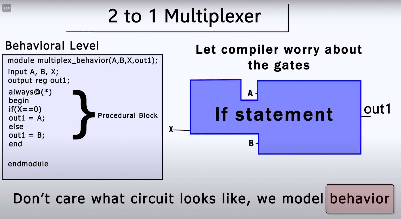
While there are features in a HDL that will be very familiar to people with coding experience, the purpose of a HDL is to describe, not to obtain a result or accomplish a task and it should not be conflated with a normal programming language. If you are curious what a HDL looks like, I recommend this video (see screenshot).
This is also the first step at which intellectual property (IP) comes in. Using IP means we don’t have to design every single part but can adopt some of them from IP providers.
After we complete our RTL code, it will undergo logic verification. This involves a series of checks that confirm the function, formal correctness and synthesisability of our chip. This can often take even more effort than the previous design stage and involves among other things detailed simulations and formal proofs.
Logic Synthesis
After we have a RTL description of our chip, we need to figure out what logic gates we need to build to turn this plan into a functioning product.
The goal here is to produce what is called a gate-level netlist. [1]The netlist contains information about what gates are included and what the connections are. There are several standard software solutions that produce the netlist for us. [2]
What information do we need to put in? Well, there is the RTL file of course, but also a Technology library file, that represents the production technology and constraint files (SDC) that describe what we are optimizing for. [3]
The first step is the actual synthesis, where we convert the RTL code into a generic logic netlist. What follows is technology mapping, where we map the abstract definitions of the gates to the standard cells of our technology library. After reaching a result we are happy with in synthesis, we conduct a variety of post-synthesis checks, often using third-party software different from the synthesis tools.[4] These checks give us initial confidence in the design before moving to the place and route stage, where more accurate analysis will be performed.
Physical Design
After we have produced a gate-level netlist that meets all our requirements, we need to specify where on the chip they should be and where all the connections are going to go.
The core of this step is another piece of software known as a place-and-route tool (PNR).[5]
Our goal here is to produce a file in GDS II format, which finally actually represents geometric shapes that the fab will end up producing. As input we of course have the gate-level netlist from the step before, but also a bunch of other files containing information about our cells and their content.[6]
The place-and-route process comprises several iterative substeps. The main components are Placing, which determines the physical locations of logic elements, and Routing, which connects these elements. Another crucial substep is Clock Tree Synthesis, which designs the clock distribution network. Each of these substeps follows a generate-check-regenerate workflow until satisfactory results are achieved, after which we proceed to the next substep.
Signoff and Tapeout
Going back to the days when literal tape was involved, the final stage is called the Tapeout. This is where you send your plans to the manufacturer.
Once the photomasks are produced, there is no way back without losing a huge amount of money. So, as you will no longer be surprised, we don’t do this without running even more tests and conducting detailed simulations to make sure everything is working as intended and all the requirements designed at the beginning are met.
Takeaways
For me the main takeaway is the huge amount of division of work. The division of the workflow into so many different steps allows engineers to effectively specialize. Having a dedicated software solution for each step basically allows the chip designer to outsource a lot of work to the makers of the software.
Some may be surprised how digital this process feels. At times it seems almost possible to forget that you are reading about hardware design. This seems relevant to me because many recent analyses of AI take-off scenarios hinge in some part on AI accelerating hardware progress. This needs a much deeper analysis by an expert in the field, but to me it seems like the way this process works makes AI induced improvements a realistic possibility. [7]
Appendix
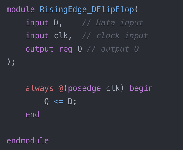
1 Verilog example
This is code in Verilog for a D Flip-Flop taken from here.
2 Gate-Level Netlist example
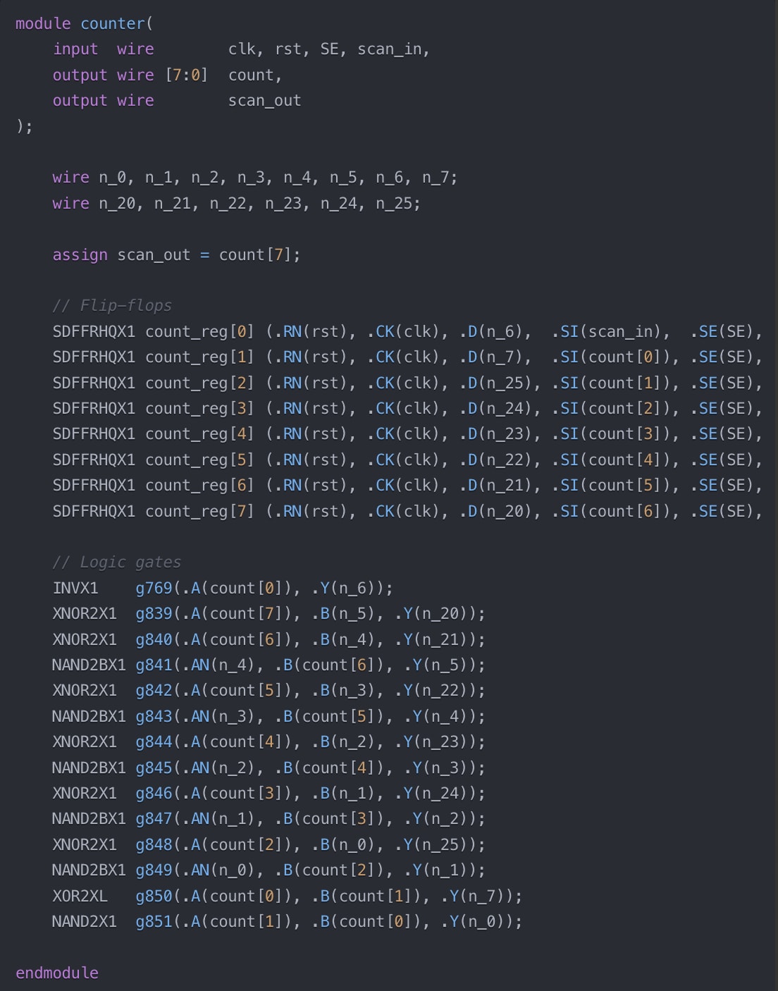
The following is an example netlist for a 8 bit counter taken from here.
Let’s look at the line
SDFFRHQX1 count_reg[0] (.RN (rst), .CK (clk), .D (n_6), .SI
(scan_in), .SE (SE), .Q (count[0]));
SDFFRHQX1 is the name of a D-Flip Flop Standard Cell chosen from the Library and and cout_reg[0] is the name of the instance. All the stuff in the brackets are the connections.
All the other bunch of letters are other Standard cells.
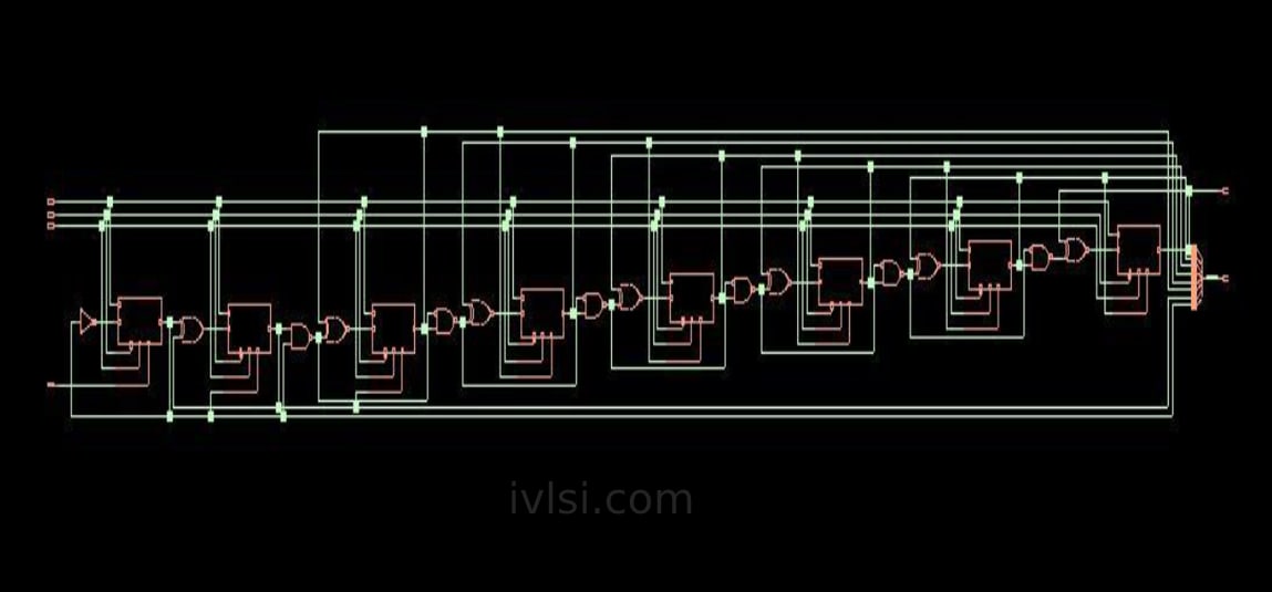
The resulting circuit looks like this
- ^
A Netlist can be flat or hierarchical. A Flat Netlist contains just one module, while a Hierarchical contains several modules that are called by the main module.
- ^
The options are Design compiler by Synopsys, Genus by Cadence and LeonardoSpectrum by Mentor Graphics
- ^
It may also include Design for testing (DFT) definitions
- ^
e.g. Gate-level simulation • Formal verification (Logic Equivalence) • Static Timing Analysis (STA) • Power/Area estimation
- ^
Here we have Innovus by Cadence, IC Compiler by Synopsys and Olympus SOC made by Mentor Graphics
- ^
So in total we have the gate-level netlist (in .V format), the multiple .lef files of our physical library, an IO assignment file (.io format), out timing library in .lib format and our constraints in the familiar .sdc format
- ^
4 comments
Comments sorted by top scores.
comment by romeostevensit · 2024-06-28T23:18:43.690Z · LW(p) · GW(p)
Physical views are somewhat interesting if you haven't seen them before https://www.youtube.com/watch?v=7d1eyZBpLn8
Replies from: Yannick_Muehlhaeuser_duplicate0.05902100825326273↑ comment by YM (Yannick_Muehlhaeuser_duplicate0.05902100825326273) · 2024-06-29T04:27:21.097Z · LW(p) · GW(p)
That's quite cool. thanks.
comment by t14n (tommy-nguyen-1) · 2024-07-01T16:43:11.633Z · LW(p) · GW(p)
Morris Chang (founder of TSMC and titan in the fabrication process) had a lecture at MIT giving an overview of the history in chip design and manufacturing. [1] There's a diagram ~34:00 that outlines the chip design process, and where foundries like TSMC slot into the process.
I also recommend skimming Chip War by Chris Miller. Has a very US-centric perspective, but gives a good overview of the major companies that developed chips from the 1960s-1990s, and the key companies that are relevant/bottlenecks to the manufacturing process circa-2022.
1: TSMC founder Morris Chang on the evolution of the semiconductor industry


